PDK Based Layout Migration
Migrating analog and mixed signal layout between foundries and processes is a complex process that must account for changes in component construction as well as new design rules.
IN2FAB's OSIRIS Layout Migration tools are designed to ported complex layout circuits while preserving the critical topology and hierarchy of the original. OSIRIS Layout Migration tools employ foundry generated PDK circuit elements to ensure the ported circuit is foundry compliant, and automatically correct by construction.
Libraries and Data
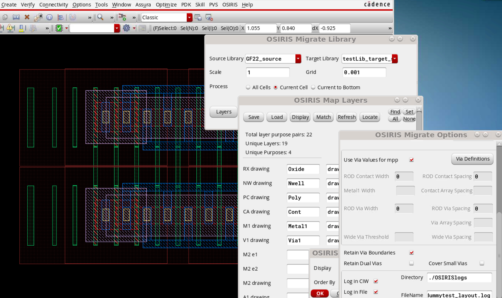
OSIRIS Layout Migration performs the complex task of translating semiconductor layout data from one foundry or process node to another. This can range from polygon level GDSII databases to highly structured PDK based circuits from advanced layout editors.
Interactive tools within OSIRIS identify the design structure and circuit elements, then guide the user through the process of translating component parameters to match new requirements.
Shape based data is adjusted and translated to new layers while advanced circuit elements such as parameterized cells and other data types are translated directly into the new circuit. Migrated components come straight from the new PDK, to ensure compatibility with the target design environment and verification tools.
Design migration takes place interactively within the layout editor, giving engineers the freedom to adjust or modify their circuit at any time. Control and processing options allow specific sections of the design hierarchy to be translated, giving users complete control over the migration process.

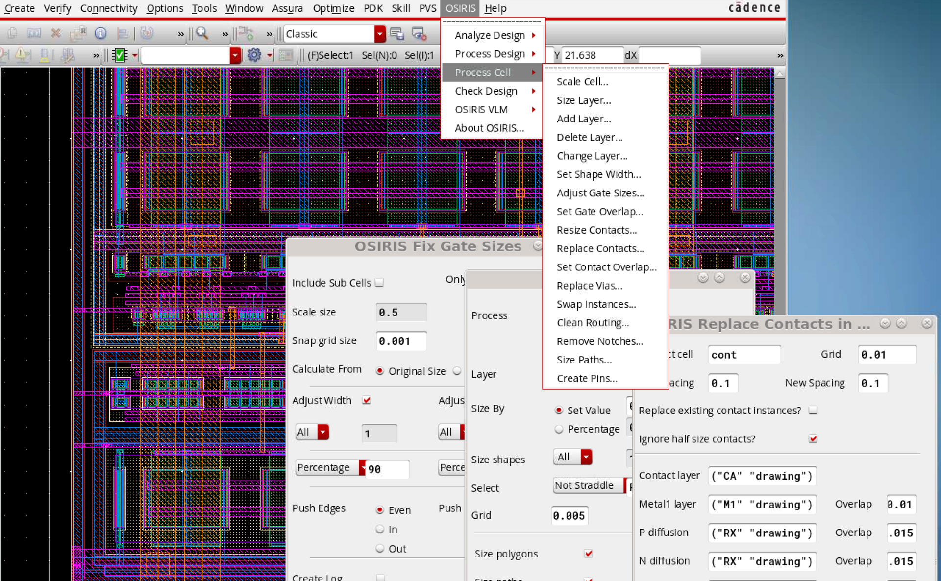
Data Mapping and Translation
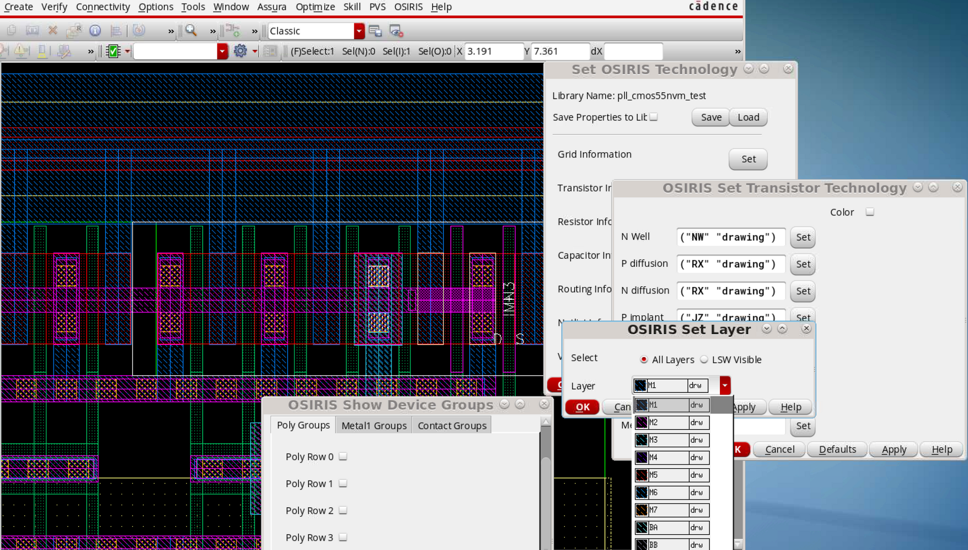
OSIRIS identifies the components in the original circuit and presents them to the user in interactive forms for mapping to the new technology. Circuit layers and parameterized cells and vias are identified and matched to equivalent sections in the new PDK. Other database elements including connectivity information and advanced layout elements are translated automatically to ensure full editing capability in the migrated layout.
Shapes, vias, guard rings and other data types are translated to new layers and adjusted to match the requirements of the new process rules. Parameterized cells are mapped to an equivalent device type from the new PDK and properties are translated and adjusted to match any new requirements.
Interactive and intuitive user interfaces search the original circuit to identify core components and help guide the user to select components form the new PDK. Physical properties can be mapped directly or automatically adjusted to resolve complicated parameter differences to generate the correct layout in the migrated design.

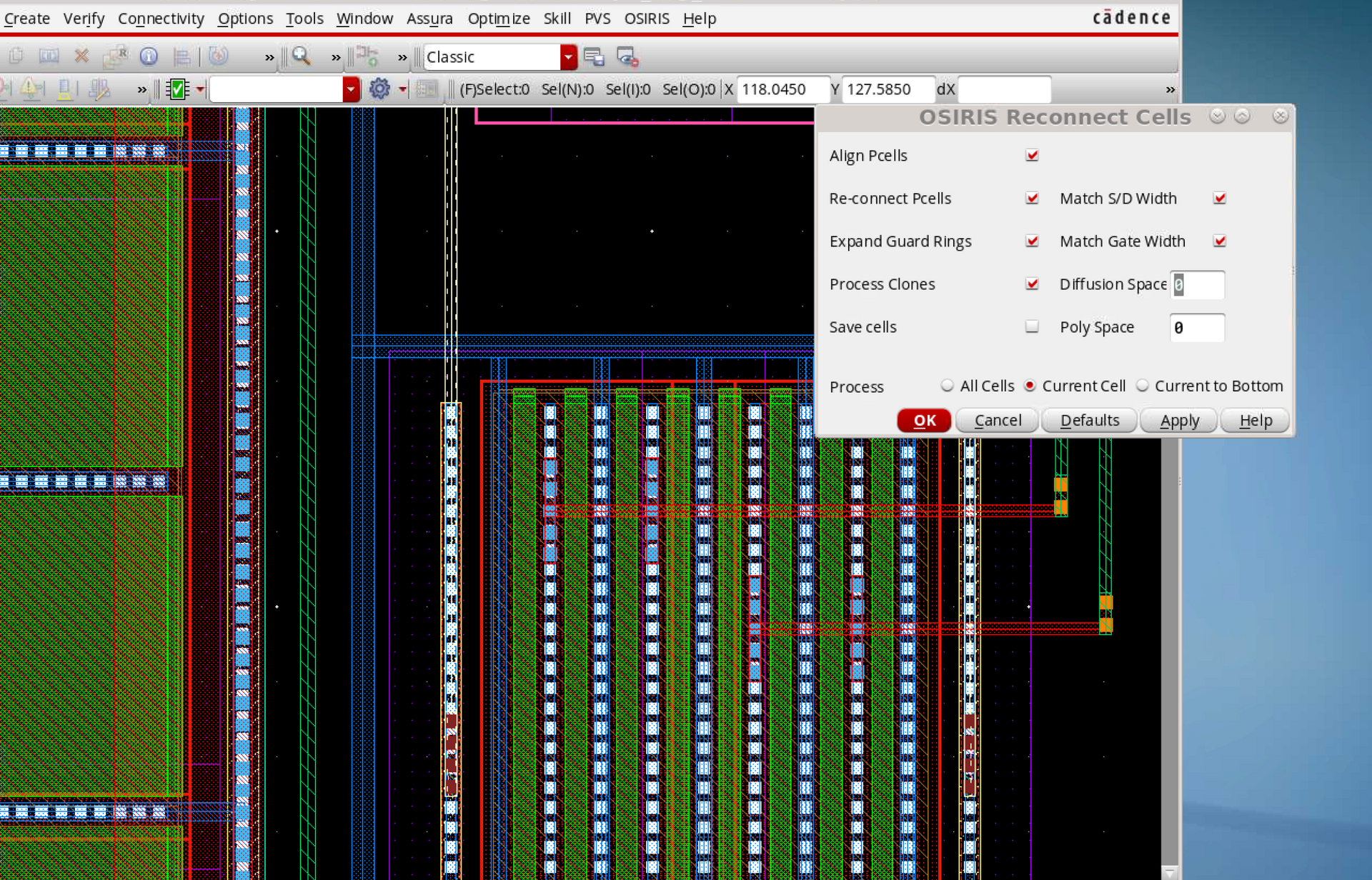
Alignment and Reconnection
Differences between the source and target design rules often mean that component placement and interconnect must be adjusted to maintain alignment and connectivity. Changes in rules such as contact size and gate spacing can mean devices become separated from overlapping cells and from routing shapes.
OSIRIS automatically recognizes the alignment and connections of components in circuits and makes small adjustments to the placement and routing in the migrated layout to align and reconnect transistors and other devices. Source and drain connections through contact overlap and wire and polygon interconnect shapes are automatically moved to retain the alignment and matching of critical devices.
OSIRIS features a host of interactive layout adjustment tools that allow users to update the circuit layout and resolve critical rules or layout requirements.
Shapes and layers can be adjusted to meet new DRC rules on single circuits or through the design hierarchy, while interactive changes can also be made at any time using a layout editor.