Schematic IP Migration
Rapid and efficient schematic migration is an essential tool for circuit porting and IP reuse. Delivering schematic databases for IP cores or full chips containing components and parameters matching the target process. Migrated schematics deliver first-level simulation results in new processes in advance of parasitic extractions from new or migrated layouts.
OSIRIS Schematic Migration features a host of features and capabilities that make it the most powerful and versatile schematic porting tool available. From legacy processes, through to the most advanced nanometer SOI and FinFET circuits, OSIRIS Schematic tools migrates the most complex designs between processes from circuit manufacturers foundries.
Libraries and Components
OSIRIS's mapping, placement, re-wiring and short location capabilities deliver full migration capability from individual circuits to complex multi-library SoC hierarchy. Circuits can be ported to a new foundry of process node in a matter of minutes, and mapping files reused for multiple migration projects.
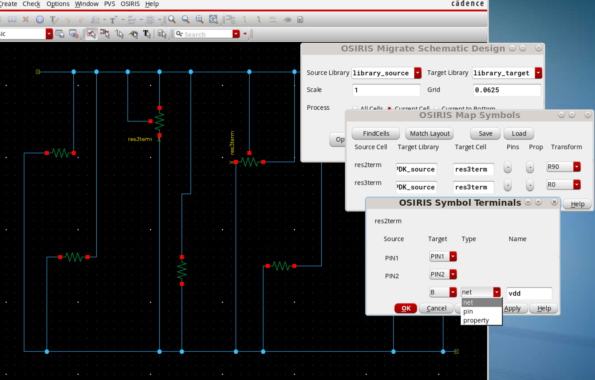
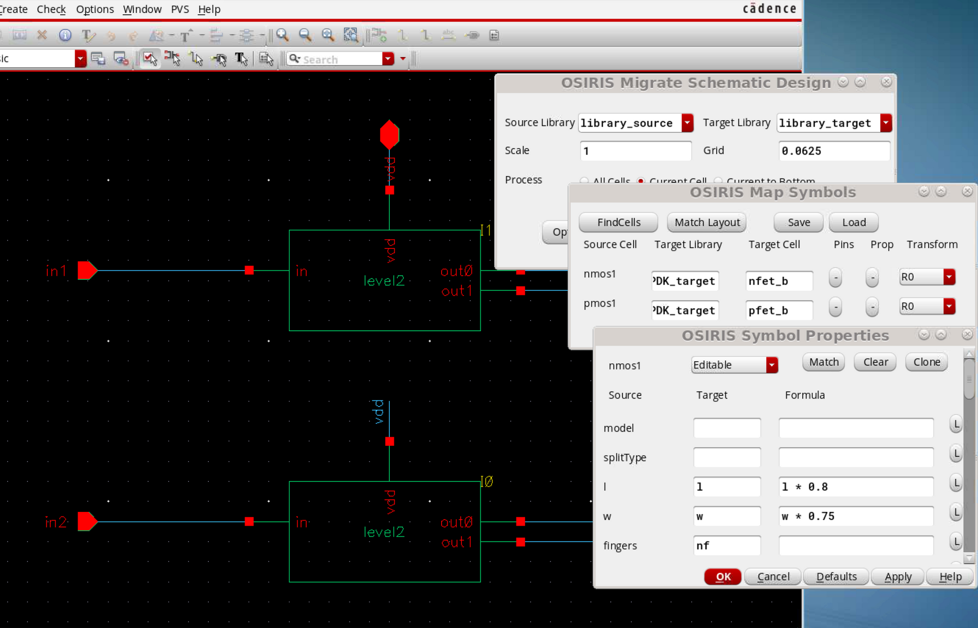
Interactive GUIs identify circuit symbols in the source design and guide the mapping of connections and parameters to the target components, while reference library cells can be replaced with equivalent versions from the new foundry.
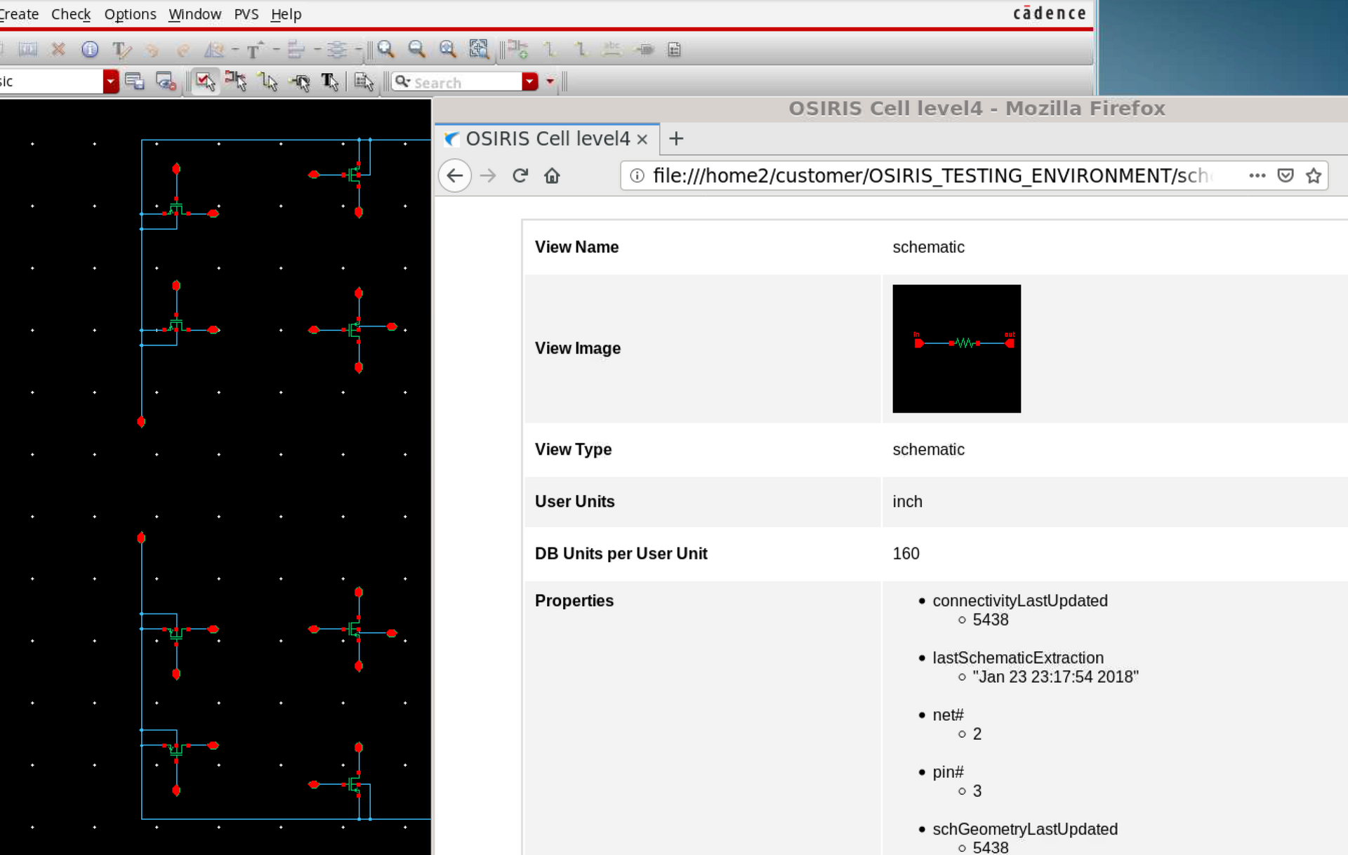
Advanced features of the schematic databases such as inherited and context-dependent parameters and properties are fully retained to deliver a completely migrated schematic containing the full functionality of the original design.
API level extensions allow the flow to be customized to meet the most demanding and intricate requirements. From complex transistor arrays to multi-level parameter calculations, OSIRIS can solve the most difficult mapping and translation challenges to rapidly port IP to new foundries and processes.

Pins and Properties
The task of mapping pins and parameters between PDKs is controlled through the OSIRIS graphical interfaces. Information from the original and new PDKs are identified and presented to the user in a clear format for easy mapping and conversion. Values can be modified by simple scaling or through complex relationships as required.
Pins are automatically rerouted to ensure connectivity even when symbols and pin positions differ and shorts caused by new pin locations are automatically identified and resolved.
Intelligent parameter assignment and callback triggers allow even the most complex components to be converted for simulation or layout constraints. Advanced commands also deal with complex demands and component modifications to resolve difficult constraints in the target process.
Comparison and API Extensions
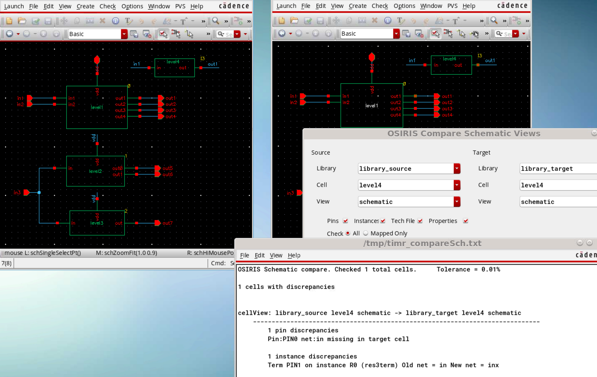
OSIRIS features a dedicated migration comparison tool that checks the placement, connectivity and parameters of the target circuit to ensure it matches the original. Schematic hierarchies are checked in a single pass with discrepancies passed back to the user for review.
Unlike an LVS tool, schematic comparison accounts for differences in component names, parameter types and values to instantly identify discrepancies between old and new circuits. Problems such as max/min size violations or component crowding are reported and highlighted within the schematic editor for easy identification.
API extensions in the Cadence Skill language can also be called to enhance the migration flow and address complex parameter and property mapping. The full lexicon of the language is available to the user, along with dedicated OSIRIS migration functions to streamline the design process.
API level extensions allow the flow to be customized to meet the demands of the most complex migration requirements. From transistor adjustments to complex parameter calculations, OSIRIS has been used to solve the most difficult mapping and translation challenges to rapidly move IP to new foundries and processes.