


Migrate Analog and Mixed-Signal Circuits Between Foundries
Reuse production proven circuits and layouts without redesign.
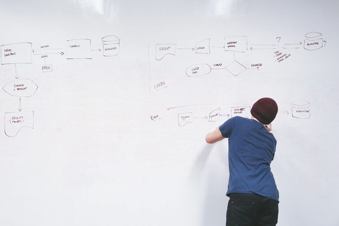
Migration Tools
IN2FAB’s OSIRIS platform automates the translation of analog and mixed-signal designs between semiconductor technologies. It converts schematics and layouts into a new process while preserving the original hierarchy and design intent, all within Cadence Virtuoso. This approach reduces months of manual redesign to just a few weeks, keeping your proven circuits production-ready in a new foundry.
OSIRIS platform enables fast and predictable migration of analog and mixed-signal IP, maximizing the reuse of proven legacy layouts and circuits. It maps devices, converts Pcells, and translates layout rules, giving engineers a reliable and repeatable workflow that maintains design integrity and minimizes risk. By dramatically shortening design and verification cycles, OSIRIS reduces engineering costs, accelerates ROI, and frees teams to focus on new IP development and innovation, all while providing secure and deterministic translation that removes uncertainty from porting.

Migration Services
When automation alone isn’t enough, our engineering team works with you to migrate your IP safely and efficiently. We handle everything from porting legacy nodes to enabling multi-foundry reuse, ensuring that performance, connectivity, and layout integrity are maintained.
Our services scale to any project size, from a single analog block to a full library of circuits. By combining our platform with hands-on engineering support, we help companies accelerate time-to-market while preserving the value of their proven designs.
By enabling IP to be reused across multiple processes and foundries, IN2FAB helps extend the commercial lifetime of existing designs and unlock new revenue opportunities. Migration allows companies to retarget proven IP for new customers, markets, and technologies without the cost and risk of full redesign, turning legacy assets into active contributors to future growth.